



Japan joins U.S. in courting investment as Samsung, SK weigh global production hubs
Sep 23, 2026, 09:40 am


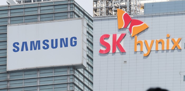 |
| Headquarters of Samsung Electronics and SK Hynix. / Yonhap |
Major economies are intensifying competition to attract investment to capitalize on the rapid growth of the artificial intelligence (AI) semiconductor market. Following the U.S., Japan is also leveraging subsidies and industrial infrastructure to draw production and R&D bases of South Korean chipmakers into its territory. For Samsung Electronics and SK Hynix, which are concurrently pursuing massive investments at home and abroad, the challenge of allocating capital, equipment, and talent while balancing technology protection and investment efficiency is growing.
Miyagi Prefecture in Japan has recently moved to attract an SK Hynix semiconductor fab, according to the Nihon Keizai Shimbun on the 22nd. An area near an industrial park housing a Toyota manufacturing subsidiary is being discussed as a candidate site. The prefecture envisions luring production facilities by capitalizing on its automotive manufacturing base, industrial infrastructure including electricity and water supplies, and Japan's ecosystem of semiconductor materials and equipment.
However, whether this will lead to actual investment remains uncertain. Miyagi Prefecture previously succeeded in attracting an 800-billion-yen semiconductor fab project from Taiwan's PSMC and Japan's SBI Holdings, only for the plan to fall through. SK Hynix also stated, "We are considering various options, including building additional production bases, to bolster our memory business competitiveness, but nothing has been decided at this point."
Samsung Electronics is likewise expanding its semiconductor footprint in Japan. The company is pursuing investment and local cooperation through the Advanced Package Lab (APL), an advanced packaging R&D base in Yokohama's Minato Mirai district. Samsung Electronics is investing roughly 40 billion yen in the APL over five years starting in 2024, with the Japanese government providing approximately 20 billion yen and the city of Yokohama offering 2.5 billion yen in subsidies.
The Japanese government has sought to rebuild its domestic chip manufacturing foundation by providing massive subsidies to TSMC's Kumamoto plant and domestic foundry Rapidus's Hokkaido facility. Its recent efforts are interpreted as an attempt to establish an end-to-end semiconductor supply chain at home by broadening the scope of its attraction efforts beyond foundries to include advanced packaging and memory.
The U.S. also stands as a primary investment destination. The U.S. government is backing local investments by both companies through subsidies and tax incentives under the CHIPS and Science Act. Key tasks include securing major anchor customers for stable operation of Samsung Electronics' Taylor fab and building a supply chain linking SK Hynix's domestic memory production facilities with its U.S. packaging base.
SK Hynix is building an advanced packaging manufacturing facility for AI memory in Indiana. Meanwhile, Samsung Electronics is constructing an advanced foundry fab in Taylor, Texas, where it recently began bringing in production equipment. After initial operations and process testing starting late this year, mass production is expected to begin in the second half of 2027.
Overseas investments offer distinct advantages, such as capitalizing on subsidies and tax incentives while improving proximity to clients as well as materials and equipment suppliers. On the other hand, dispersing production and R&D bases across multiple regions can drive up capital expenditure and increase the burden of securing advanced equipment, skilled talent, and core technology protection.
An industry official remarked, "As massive investments proceed simultaneously at home and abroad, clearly delineating the role of each base is essential. Companies must take into comprehensive account not only the scale of incentives, but also customer accessibility, technology safeguards, and the acquisition of specialized talent."
Lee Ji-sun
Most Read
-
1
Celltrion’s Omlyclo gains ground in major European..

-
2
Trump demands rates fall below 1% as Fed hikes for..

-
3
Trump makes $1 trillion bet ahead of midterm elect..

-
4
Iran resumes ballistic missile production, assembl..

-
5
Trump warns countries not helping U.S. must pay re..

-
6
Apple launches first foldable, 1 million won prici..

-
7
Turkish Airlines named main club partner of Liverp..

PEOPLE







-
Address : In-Young Bldg., 34, Uisadang-daero 1-gil, Yeongdeungpo-gu, Seoul
Copyright by ASIATODAY CO., LTD. All rights resereved