

Hanmi Semiconductor launches FC Bonder 3.5 for AI system semiconductors
Jun 26, 2026, 09:41 am


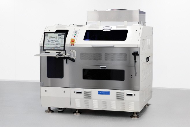 |
| Hanmi Semiconductor's FC Bonder. / Courtesy of Hanmi Semiconductor |
Hanmi Semiconductor announced on the 26th that it has launched its new equipment, "FC Bonder 3.5 (FLIP CHIP BONDER 3.5)," for AI system semiconductors and will supply it to global foundry and Outsourced Semiconductor Assembly and Test (OSAT) companies.
Hanmi Semiconductor currently ranks first globally in the market for TC bonders used in High Bandwidth Memory (HBM). Moving forward, the company intends to expand its presence into the 2.5D packaging market, which is widely utilized in system semiconductors.
To address the rapidly growing 2.5D packaging market fueled by surging demand for AI chips, Hanmi Semiconductor developed the FC Bonder 3.5 following the launch of the FC Bonder 75 last year. The rollout expands its product lineup designed to support extra-large dies and multi-chip integration processes, which are critical for implementing AI semiconductors.
Presently, the 2.5D packaging process has established itself as a foundational technology in AI semiconductors and High-Performance Computing (HPC). This expansion is driven by global big tech companies—including Nvidia, AMD, Broadcom, Marvell, and Apple—actively adopting the technology to manufacture their proprietary AI chips.
Hanmi Semiconductor's FC Bonder 3.5 satisfies the latest processing standards demanded by global AI semiconductor firms. It delivers significantly enhanced productivity and precision compared to competing systems, and applies a Chip-to-Wafer (C2W) bonding method to integrate 2.5D logic dies, enabling the processing of large panels and substrates up to 340mm in size.
Recently, as high-performance AI chips evolve toward Panel-Level Packaging (PLP) formats, they are advancing into multi-die (chiplet) structures that integrate multiple chips—such as GPUs, CPUs, and HBM—into a single package. Consequently, substrates measuring 250mm and 310mm have become the mainstream in AI packaging processes. The FC Bonder 3.5 is engineered to align with this demand, reliably supporting clients' next-generation AI semiconductor production.
Furthermore, alongside flip-chip bonding, the FC Bonder 3.5 features a face-up (non-flip) bonding function that utilizes Die Attach Film (DAF) materials. This dual capability allows the machine to adapt flexibly to varying processing conditions across different customers.
Concurrently with its expanded product lineup, Hanmi Semiconductor will establish a local U.S. subsidiary, "Hanmi USA," late this year to sharply strengthen its regional sales and customer service capabilities. The move serves as a strategic framework to expand its client base across all fronts in the U.S. market, home to dominant big tech firms, by supplying foundries and OSAT providers with both HBM TC bonders and system semiconductor manufacturing equipment.
"Building on our bonding technical expertise proven through HBM TC bonders, we aim to deliver milestones that will substantially contribute to our revenue in the emerging 2.5D packaging market," a Hanmi Semiconductor official stated. The official added, "We will continuously roll out advanced packaging solutions required in the era of AI semiconductors."
Lee Ji-sun
Most Read
-
1
FBI foils terror plot against Trump’s White House..

-
2
Iran to allow IAEA inspectors back for uranium dis..

-
3
Chinese tourists' resumption of travel to Japan fa..

-
4
Japan, UK issue joint economic security declaratio..

-
5
Iran’s IRGC attacks cargo ship in Strait of Hormuz..

-
6
Trump mulls $300bn Iran rebuild fund with potentia..

-
7
U.S.-Iran sign final MOU, released by U.S. media

PEOPLE


-
Address : In-Young Bldg., 34, Uisadang-daero 1-gil, Yeongdeungpo-gu, Seoul
Copyright by ASIATODAY CO., LTD. All rights resereved