



Samsung proves tech leadership with first 7th-gen HBM samples
May 29, 2026, 03:51 pm


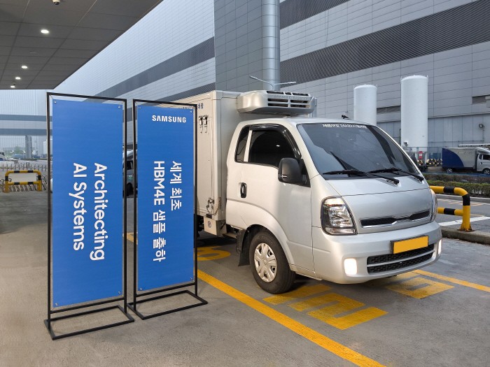 |
| /Samsung Electronics. |
Samsung Electronics has reinforced its semiconductor technological edge by becoming the first in the world to ship samples of its seventh-generation High Bandwidth Memory (HBM), designated as HBM4E. The development comes just three months after the company successfully initiated mass-production shipments of its sixth-generation HBM4 in February, sharply elevating market expectations for a substantial rebound in Samsung's global HBM market share. Following this initial sample deployment, Samsung plans to scale up to full commercial mass production of HBM4E aligned with its clients' launch timelines.
Samsung announced on May 29 that it has commenced the supply of 12-layer HBM4E samples to global customers. While the tech giant did not explicitly name its clients, industry insiders strongly indicate that the shipments were delivered to Nvidia, widely considered the primary anchor client in the artificial intelligence hardware ecosystem. Samsung’s rapid transition follows its industry-first mass-production shipment of HBM4 earlier this February. "This HBM4E deployment transcends a simple expansion of our product catalog," a Samsung representative explained. "It serves as a structural milestone that cements our unparalleled supply capabilities and technological dominance in the global AI infrastructure market, which is projected to experience exponential growth over the coming years."
According to technical specifications released by Samsung, the operational speed per pin on the HBM4E ranges from 14 Gbps up to a maximum of 16 Gbps, marking a performance leap of over 20% compared to its predecessor. Generating a processing bandwidth of up to 3.6 TB per second on a single stack, the architecture is engineered to maximize computing velocities for Large Language Models (LLMs) and next-generation AI processing units. Capacity thresholds have similarly been expanded; the 12-layer HBM4E achieves a high-density capacity of 48 GB, yielding a 30% volume increase over prior iterations. Moving forward, Samsung intends to diversify its portfolio into 32 GB (8-layer) and 64 GB (16-layer) configurations to support highly customized enterprise operational environments.
The newly unveiled HBM4E integrates Samsung's proven, cutting-edge 1c-nanometer (sixth-generation 10nm-class) DRAM alongside a proprietary 4-nanometer logic die fabricated via its in-house foundry. This hardware fusion maximizes sub-microscopic process stability while simultaneously securing optimal manufacturing yields and volume production viability. Furthermore, by incorporating low-power architectural blueprints and advanced packaging optimization techniques, the HBM4E achieves a 16% improvement in overall energy efficiency alongside a 14% reduction in thermal resistance characteristics compared to earlier models.
Backed by these technological competitive advantages, Samsung's strategic positioning within the broader HBM merchant market is anticipated to expand rapidly. By accelerating its sample shipment timeline ahead of key competitors, the company has positioned itself favorably to lock in volume commitments from major hyperscale clients. According to data from market tracker Counterpoint Research, Samsung occupied the second position in the global HBM market with a 22% share in the fourth quarter of last year, trailing SK Hynix's 57% market dominance. While this represents a noticeable contraction from the 40% share recorded a year prior, the commercial rollout of HBM4 this year is providing a strong foundation for an aggressive market rebound.
In institutional evaluations, global technology clients have consistently returned highly favorable feedback regarding the aggregate performance, processing speeds, and power efficiency metrics of Samsung’s HBM4 lineups. In December of last year, Samsung’s HBM4 achieved top-tier ratings during its final System-in-Package (SiP) validation phase, demonstrating an industry-leading speed of 11.7 Gbps. Given that mass production is already underway for HBM4 architectures utilizing the identical 1c DRAM and 4nm base die matrix, market analysts evaluate that the newly introduced HBM4E is highly likely to achieve an exceptionally compressed timeline toward full mass-production status.
Financial analysts maintain a decidedly bullish outlook on Samsung's memory division trajectory. "The structural supply deficit in the global memory market is projected to intensify significantly into 2027, amplifying upward pricing momentum," noted Kim Dong-won, a senior research analyst at KB Securities. "Crucially, ongoing contractual negotiations for HBM are actively factoring in the narrowing margin differentials between HBM and conventional commodity DRAM, paving the way for a projected price surge of over 50% year-over-year."
Hwang Sang-jun, Executive Vice President and Head of Memory Development at Samsung Electronics, emphasized the strategic weight of the milestone. "Following our successful execution of HBM4 mass production, the seamless delivery of our next-generation HBM4E samples firmly stamps Samsung's undisputed technological leadership onto the global marketplace," Hwang stated. "Moving forward, we will continue to aggressively spearhead the expansion of the global AI memory ecosystem, anchored by our overwhelming technological super-gap and proactive capital investments in foundational production infrastructure."
Yeon Chan-mo
Most Read
-
1
Kia Sportage outperforms Mazda CX-5 in German auto..

-
2
Houthis launch successive attacks on Saudi airport..

-
3
Saudi Arabia, Iran hold first diplomatic talks to..

-
4
U.S. deploys carrier, 10,000 more troops to Middle..

-
5
Saudi airport in Riyadh struck again, leaving at l..

-
6
Putin's ally visits China on the 8th ahead of APEC..

-
7
Chinese military support and training center opens..

PEOPLE






HEADLINE NEWS

-
Address : In-Young Bldg., 34, Uisadang-daero 1-gil, Yeongdeungpo-gu, Seoul
Copyright by ASIATODAY CO., LTD. All rights resereved