



SK Hynix builds HBM production base in Indiana, U.S.
Aug 28, 2026, 09:06 am


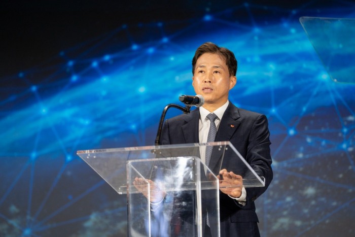 |
| SK Hynix CEO Kwak Noh-jung announces business strategies and vision at a groundbreaking ceremony for an AI memory production facility held at Purdue University in West Lafayette, Indiana, U.S., on the 27th (local time). / SK Hynix |
SK Hynix is establishing a next-generation High Bandwidth Memory (HBM) production base in the U.S. Observers note that the move carries great significance as it ushers in a new future for South Korea-U.S. cooperation in artificial intelligence (AI).
On the 28th, SK Hynix announced that it held a groundbreaking ceremony the previous day (local time) for an advanced packaging production facility for AI memory at Holloway Gymnasium at Purdue University in West Lafayette, Indiana, U.S. Advanced packaging is a cutting-edge backend semiconductor technology that bundles or vertically stacks multiple chips to enhance performance, overcoming the physical limitations of scaling down chip size through miniaturization processes.
From the U.S. side, key political and government figures attended the groundbreaking ceremony, including Indiana Governor Mike Braun and U.S. Senator Todd Young, alongside Purdue University President Mitch Daniels and Chairman of the Korea Defense Veterans Association Robert Abrams. From South Korea, South Korean Ambassador to the U.S. Kang Kyung-wha, SK Group Vice Chairman for U.S. Operations Yu Jeong-joon, Vice Chairman Lee Hyung-hee, and SK Hynix CEO Kwak Noh-jung were present.
The Indiana fab, representing a total investment of more than 4 billion dollars, is scheduled to complete its cleanroom in October 2028 and begin mass production of next-generation HBM in the second half of 2029. An SK Hynix official explained that once production enters full swing, it will grow into a core HBM production hub in the U.S. led by a workforce of around 1,000 personnel.
SK Hynix particularly emphasized that as its first HBM production outpost established in the U.S., the facility features an integrated production system operating in close connection between South Korea and the U.S. Under this structure, cutting-edge wafers manufactured in South Korea will be transported to Indiana, where they undergo advanced packaging and testing before "Made in USA" HBM products are supplied to U.S. clients.
The company also noted that tangible investments are accelerating in earnest following its American Depositary Receipt (ADR) listing, contributing to stabilizing the U.S. semiconductor supply chain and bolstering national security and economic strength.
"Currently, more than 100 partner companies in materials, parts, and equipment are discussing entering West Lafayette," an SK Hynix official stated. "This is expected to support the stable operation of the Indiana fab and further solidify the U.S. AI ecosystem." The official added, "Through the construction and operation of the fab, we plan to create about 7,000 direct and indirect jobs alongside U.S. companies."
On the same day, SK Hynix also signed a memorandum of understanding with Purdue University for research and development cooperation in advanced packaging.
Under this agreement, the two sides will jointly research advanced packaging and next-generation system integration technologies, including HBM. SK Hynix also plans to expand cooperation with major universities and research institutions across the U.S. Midwest to focus on cultivating and recruiting top-tier global talent.
"Today marks the day when the U.S. and SK Hynix begin a new future of AI together," SK Hynix CEO Kwak Noh-jung said. "The U.S. is the epicenter of AI innovation where premier clients, research capabilities, and ecosystems converge, and the Indiana fab will serve as the base providing the first 'Made in USA' HBM." He added, "We will expand our investment and collaboration in the U.S., grow together, and become the most trusted partner shaping the future of U.S. AI."
Choi In-gyu
Most Read
-
1
Kia Sportage outperforms Mazda CX-5 in German auto..

-
2
Houthis launch successive attacks on Saudi airport..

-
3
Saudi Arabia, Iran hold first diplomatic talks to..

-
4
U.S. deploys carrier, 10,000 more troops to Middle..

-
5
Saudi airport in Riyadh struck again, leaving at l..

-
6
Japan tracks Ukraine fiber-optic drones, bolsters..

-
7
Putin's ally visits China on the 8th ahead of APEC..

PEOPLE





HEADLINE NEWS
- Trump slams Nobel Peace Prize snub, claiming he is 'preventing war' between the two Koreas
- China makes tactical retreat following fierce pushback from EU
- Japan openly opposes U.S. sanctions on ICC, fueling tensions with Washingto..
- Military service exemptions for artists and athletes under scrutiny at parl..

-
Address : In-Young Bldg., 34, Uisadang-daero 1-gil, Yeongdeungpo-gu, Seoul
Copyright by ASIATODAY CO., LTD. All rights resereved