 |
AsiaToday reporter Hong Sun-mi
Taiwan Semiconductor Manufacturing Company (TSMC) has begun to solidify its position as the world’s biggest contract chipmaker by reviewing building its chipmaking plant in Japan.
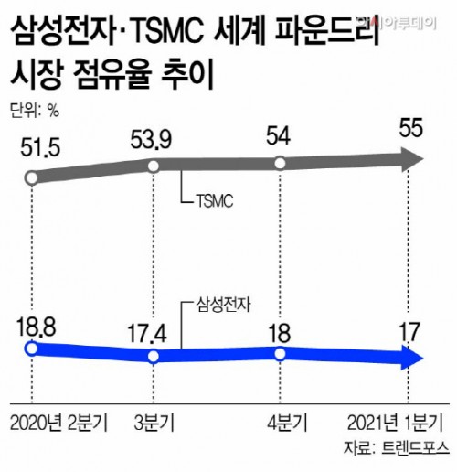
Industry observers say TSMC’s latest move is similar to Samsung Electronics’ super-gap strategy by beating out competitors through massive investment in facility and technology development. On the other hand, Samsung Electronics is delaying its decisions on large investments due to the absence of Vice Chairman Lee Jae-yong, raising concerns that the gap with TSMC could widen further.
According to industry sources on Friday, the Nihon Keizai Shimbun reported Friday that TSMC is evaluating plans to build a plant in Kumamoto Prefecture, in western Japan.
Earlier, Japanese media outlets reported TSMC had decided to open a research and development facility in Tsukuba, Ibaraki Prefecture, and that the Japanese government would subsidize about 19 billion yen. If investments are made in both Ibaraki and Kumamoto prefectures, TSMC would have research and production facilities in Japan.
TSMC has been aggressively expanding its semiconductor presence, taking advantage of the countries’ movements to expand their semiconductor supply chain amid the growing market.
TSMC recently announced that it would build a total of six foundry facilities, including one in Arizona, USA. Considering that it costs around 13 trillion won (US$11.6 billion) to a single facility in Arizona, industry observers expect that TSMC’s facility investment in Arizona would reach about 80 trillion won (US$71.6 billion).
In April, TSMC announced its plan to spend $100 billion over the next three years, in addition to its previous plan announcement to invest $28 billion this year. It means that the chipmaker plans to invest more than $30 billion annually in foundry facility investment for the next four years.
On the other hand, Samsung Electronics’ investment is relatively cautious. At the South Korean government’s announcement of the K-Semiconductor strategy last month, Samsung announced that it would increase its investment to 171 trillion won (US$151 billion) from 133 trillion won to achieve its goal of becoming the world’s No.1 logic chip maker by 2030. It means that the company plans to annually invest about 15 trillion won (US$13 billion) in system semiconductors such as foundries by 2030, which is less than half of TSMC’s investment which is pouring nearly 40 trillion won (US$38 billion) annually.
Samsung has revealed its $17 billion investment plan in the United States during the Seoul-Washington summit, but is yet to choose a location for the new facility. It has not confirmed the size of the facility for its Pyeongtaek plant in Gyeonggi Province. In addition, Samsung Electronics is falling behind TSMC in terms of operating profit and technology.
#TSMC #Samsung Electronics #foundry
Copyright by Asiatoday
Most Read
-
1
-
2
-
3
-
4
-
5
-
6
-
7


