

Samsung begins mass production of world’s first 3-nm chips
Jul 01, 2022, 09:30 am


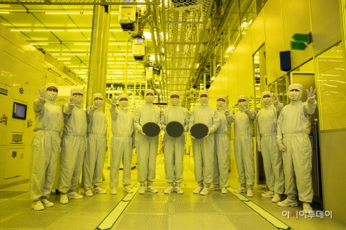 |
| Samsung Electronics executives hold 3-nanometer wafers at the company’s production line in Hwaseong, Gyeonggi Province, along with workers holding up three fingers to celebrate the world’s first mass production of 3-nanometer chips./ Source: Samsung Electronics |
AsiaToday reporter Choi Won-young
Samsung Electronics has begun mass production of the world’s first 3-nanometer semiconductions. One nanometer is one-millionth of a millimeter and a strand of human hair is around 100,000 nanometers wide. Compared to conventional 5-nanometer chips, the newly developed 3-nanometer process can reduce power consumption by up to 45 percent, improve performance by 23 percent, and reduce surface area by 16 percent. When installed in high-performance, low-power system semiconductors or mobile chips, its innovative technology is expected to enhance the competitiveness of products greatly.
The industry evaluates that Samsung’s 3-nanometer mass production is a winning move to beat its rival and foundry leader TSMC, which occupies 53 percent of the global market, and supporting evidence that Samsung’s technology could change the chip market.
According to Samsung Electronics on Thursday, the 3-nanometer chips are built on Gate-All-Around (GAA) technology, which was introduced to overcome the issue of lowered power efficiency, which is considered the biggest obstacle of ultra-fine processes.
The so-called ‘Moore’s law, which states that the number of transistors on a microchip double about every two years, started to go against in the 2010s. In particular, the existing semiconductor industry had claimed that they have reached their limit when they reached the mass production of 4-nanometer process. For this reason, the industry evaluates that Samsung’s 3-nanometer chips can become a ‘game changer’ as the next-generation foundry market. Samsung Electronics also plans to develop the second-generation 3-nanometer process using GAA to reduce power consumption by up to 50 percent, improve performance by 30 percent, and reduce surface area by 35 percent.
Samsung plans to increase its number of clients to around 300 by 2026 from 100 in 2021. “Samsung Electronics has grown rapidly as we continue to demonstrate leadership in applying next-generation technologies to manufacturing, such as the foundry industry’s first high-K metal gate, FinFET, as well as extreme ultraviolet (EUV) lithography,” said Choi Si-young, head of the company’s foundry business. “We will continue active innovation in competitive technology development and building processes that help expedite achieving the maturity of technology.”
#Samsung #3 nanometer #chip #mass production #TSMC
Copyright by Asiatoday
Most Read
-
1
Heung-min Son says "I'm sorry," but fans..

-
2
Iran's IRGC launches airstrikes on U.S. military f..

-
3
Netanyahu requests Trump to halt F-35 sales to Tur..

-
4
Japan invests 2 trillion yen in India to shift chi..

-
5
Khamenei's two-day funeral: Three sons spotted, su..

-
6
Trump imposes new Iran blockade and 20% Hormuz tol..

-
7
Samsung Electronics sets record with 89.4 trillion..

PEOPLE


-
Address : In-Young Bldg., 34, Uisadang-daero 1-gil, Yeongdeungpo-gu, Seoul
Copyright by ASIATODAY CO., LTD. All rights resereved