



AI chip battleground shifts from computation to interconnection as Samsung and SK bet on packaging
Aug 23, 2026, 10:15 am


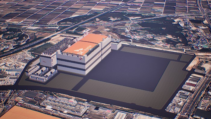 |
| A rendering of SK Hynix's Cheongju P&T7. / SK Hynix |
The performance competition in AI semiconductors is expanding beyond improving computing power through fine fabrication processes to how quickly and efficiently memory and computing chips are connected. As computing performance of AI accelerators rises rapidly while memory bandwidth and inter-chip data transfer speeds fail to keep pace, advanced packaging has emerged as a key technology to resolve this new bottleneck. Samsung Electronics and SK Hynix are also expanding related investments and technology development.
According to Counterpoint Research on August 20, more than 130 million graphics processing units (GPUs) and application-specific integrated circuits (ASICs) for AI servers are projected to be shipped packaged with memory through advanced packaging over the next five years. Computing revenue generated on this basis is expected to reach approximately 2 trillion dollars.
The forecast indicates that as computing speeds of AI semiconductors accelerate, bottlenecks—where memory data delivery speeds cannot keep pace or data movement between chips is delayed—are occurring, making advanced packaging even more important.
Currently, the advanced packaging ecosystem is led by TSMC with its Chip-on-Wafer-on-Substrate (CoWoS) technology. This method connects GPUs and High Bandwidth Memory (HBM) on a single package using a silicon interposer, and it has established itself as the leading technology following its adoption by Nvidia.
Intel is also pursuing the development of next-generation technologies such as ZAM and XBM to reduce data bottlenecks between memory and computing chips, following its EMIB method, which uses silicon bridges inserted between chips for interconnection. Last June, the company recruited former SK Hynix CEO Lee Seok-hee to oversee the development and manufacturing of advanced packaging and back-end process technologies, strengthening its capabilities in this area.
Domestic companies are also accelerating efforts to strengthen packaging competitiveness. Samsung Electronics is reinforcing its turnkey strategy of offering HBM, foundry services, and advanced packaging together. Through cooperation with Broadcom to build next-generation AI infrastructure, the company expanded its scope of collaboration beyond HBM and sub-2-nanometer foundries to include 2.3D and 2.5D advanced packaging. With demand for AI and data centers rising, customer demand to secure both memory and foundry capacity simultaneously is expected to grow further.
SK Hynix is investing approximately 19 trillion won in Cheongju to construct P&T7, an advanced packaging production facility, while also establishing an advanced packaging production and R&D base for HBM in Indiana, U.S. The plan is to secure packaging production capacity in response to the increasing stacking layers of HBM and growing demand for AI memory.
In parallel, research is also underway on next-generation interconnection technologies to eliminate data movement bottlenecks between chips. On this day, SK Hynix unveiled a Co-Packaged Optics (CPO) technology roadmap in the international academic journal Nature Electronics alongside global researchers, integrating optical transceivers with processors in a single package.
As such, industry observers expect the importance of packaging to increase further going forward as AI semiconductors become higher performing and HBM stacks higher. The analysis suggests that not only computing performance improvements through fine fabrication processes, but also technologies that efficiently connect memory and computing chips to boost data transfer speeds and power efficiency, are establishing themselves as core pillars of AI semiconductor competitiveness.
Lee Ji-sun
Most Read
-
1
Trump shares map on social media labeling Strait o..

-
2
Kia Sportage outperforms Mazda CX-5 in German auto..

-
3
Houthis launch successive attacks on Saudi airport..

-
4
U.S. deploys carrier, 10,000 more troops to Middle..

-
5
Trump rejects Iran's offer to open Strait of Hormu..

-
6
N. Korea conducts first swarm attack drill with dr..

-
7
U.S.-China summit falls short on substance as Trum..

PEOPLE






HEADLINE NEWS
- Seoul dismisses Ukraine's claim of 'S. Korean support for Russia' as "inaccurate and inappropriate"
- S. Korea, Japan race to develop nuclear-powered submarines
- Henri Kagan, Kenso Soai win Nobel Prize in Chemistry for uncovering how mol..
- Vance says Alaska LNG cooperation will move forward with Seoul's current or..

-
Address : In-Young Bldg., 34, Uisadang-daero 1-gil, Yeongdeungpo-gu, Seoul
Copyright by ASIATODAY CO., LTD. All rights resereved