

SK hynix unveils world’s first 321-layer NAND
Aug 10, 2023, 10:41 am


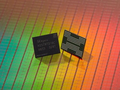 |
| SK hynix unveiled its 321-layer NAND memory. / Courtesy of SK hynix |
AsiaToday reporter Woo Sung-min
Korean chipmaker showed off its super-gap technology to the world at Silicon Valley, the heart of the world high-tech industry. It seems that the chipmaker has overcome the semiconductor recession with its core technology and is preparing for the upcoming super-cycle.
SK hynix unveiled the world’s first memory that exceeds 300 layers in the NAND flash area, where higher the number of layers means the better performance and efficiency. Samsung Electronics also introduced a number of next-generation memory solutions, including solid state drives (SSDs) for the 8th-generation V-NAND-based data centers.
At the Flash Memory Summit 2023 held in Santa Clara, California, SK hynix unveiled samples of the world’s first 321-layer 1 terabit TLC 4D NAND Flash and made public the progress on its development. The chipmaker has nearly doubled the number of layers in just two years since its mass-production of the 176-layer chips. It plans to start mass production from the first half of 2025.
“The success in producing the 238-layer NAND has helped the smooth progress for the development of the 321-layer product,” an official from SK hynix said, adding, “With another breakthrough to address stacking limitations, SK hynix will open the era of NAND with more than 300 layers and lead the market.” Five or six years ago, chip experts had predicted 200 layers as the limit of stacking, however SK hynix began mass-producing 238-layer chips this year and succeeded in stacking more than 300 layers this time.
Unlike DRAM, where data is fully volatilized, NAND flash is a memory where data remains stored even when the power is turned off. For NAND, the technology of vertically stacking cells, the basic storage unit, is important because the higher the number of layers stacking, the more data can be stored in a narrow area and therefore reducing power consumption. Stacking more cells and larger storage capacity on a single chip means the total capacity that can be produced on a single wafer is increased.
Although high-stacking NAND does not necessarily mean an unconditional performance advantage due to differences in process methods among companies, the industry sees it as one of the important keys to lowering manufacturing costs in the long run and accelerating the replacement of HDDs.
“The higher the number of layers, the more capacity and the better NAND flash works,” said Kang Sung-chul, a researcher at the Korean Society of Semiconductor & Display Technology. “This is why NAND flash companies are struggling to compete for stacking layers.”
#SK hynix #layer #NAND #flash #chip
Copyright by Asiatoday
Most Read
-
1
Gov’t to extend fuel tax cut by 2 months amid Midd..

-
2
Finance ministers of S. Korea, U.S., Japan recogni..

-
3
Gov’t to set up a special presidential committee o..

-
4
Yoon appoints new chief of staff to boost communic..

-
5
Tax authorities launch probe into wholesalers amid..

-
6
2nd working-level consultation over Yoon-Lee meeti..

-
7
NCT Doyoung to release “YOUTH” today

PEOPLE


-
Address : In-Young Bldg., 34, Uisadang-daero 1-gil, Yeongdeungpo-gu, Seoul
Copyright by ASIATODAY CO., LTD. All rights resereved